As an example, António Costa pointed to an amount of one billion euros for the mobilizing agendas included in the Recovery and Resilience Plan, “with the potential to grow another 12 billion euros if there is capacity and effective demand for its use”.
In addition to natural resources, such as lithium, and funding, the Prime Minister highlighted another advantage that he considers Portugal to have in this energy transition process, which is “knowledge”.
INL: Preventive measures and Contingency Plan regarding COVID-19 [ UPDATE ]

The INL – International Iberian Nanotechnology Laboratory has been implementing internal measures since the end of last January to limit the spread of the new Coronavirus also known as COVID-19 and has elaborated a Contingency Plan, in compliance with orientations from the DGS (Portuguese Health Authority).
These preventive measures are focused on society at large by safeguarding both our employees to get infected as well as reducing the possibility that our employees would serve as agents for further spread. The measures follow the recommendations of the World Health Organization and the Health General-Directorate of Portugal, where INL is headquartered.
We have formed a COVID-19 Safety Commission consisting of the Director-General, Chief Administration Officer, Chief Site Management Officer, Coordination & Quality Manager, Legal Service Manager, Corporate Communication & Marketing Manager, Health, Environment and Safety Officer, and the Director-General Executive Assistant.
We have developed a contingency plan to be activated if any suspected cases of COVID-19 are detected.
The following measures are presently in force at INL:
-
INL employees are being advised to strictly adhere to WHO recommendations such as frequently wash their hands, as this is the most effective way to limit the spread of the COVID-19 virus.
-
All the events organised at INL and school visits to our facilities are cancelled until further notice.
-
INL Guest House is closed until further notice.
-
INL is also avoiding, as much as possible, physical participation in internal and external meetings, using digital tools in alternative and remote work is being adopted to limit exposure as much as possible.
-
When digital means are not available, duty travel on behalf of INL is authorised to certain areas.
The use of a face mask to enter INL premises is mandatory for all, including INL suppliers, contractors’ personnel, start-up members, technical visitors, authorised family members, and it must be used at all times indoor or outdoor, until leaving INL Campus
-
INL encourages remote work for all functions and activities that can be performed remotely.
-
All members of the personnel are quarantined for 14 days after a possible encounter and/or if coming from an area outside a circle with a radius of 200 km with its centre at INL premises.
Regarding the Contingency Plan, it applies to the whole INL community: Members of the Personnel, Contracted Personnel, Institutional, and other Visitors.
The goals of the INL Contingency Plan for Covid-19 are:
-
To determine the needs and resources for an effective response proportional to the risk level;
-
To communicate and make known any reliable and updated information to the INL Community;
-
To implement primary prevention measures, suitable for any current risk level;
-
To precociously detect any illness cases and their respective contacts, ensuring a responsive connection to the appropriate health services;
-
To ensure a coordinated response with other institutions and organizations;
-
To ensure the continuity of INL activity, according to the risk level;
-
To minimize the effect of the pandemic within the INL community.
Its application is to be dynamic and changeable under new information or with any new facts that may arise. These may lead to new measures and result in the plan’s update.
You can download the full document regarding the Contingency Plan by clicking here.
Remember, protect yourself and your community from getting and spreading COVID-19. Everyone has a role to play in getting ready and staying healthy.
INL approves its Gender Equality Plan and the INL Respectful Workplace Policy
The INL – International Iberian Nanotechnology Laboratory has approved its internal Gender Equality Plan and the INL Respectful Workplace Policy.
The two documents that have now entered into force demonstrate INL’s commitment to achieving gender balance and equality by establishing clear goals, detailed actions, and measures. They also include a statement of INL’s pledge to prevent and intervene in every situation of discrimination, harassment, or abuse of authority.
By approving these two official regulations, INL aims to address its internal and external community with a strong statement, making INL an even better place to work and maximising the potential of nanotechnology research for the benefit of global society.
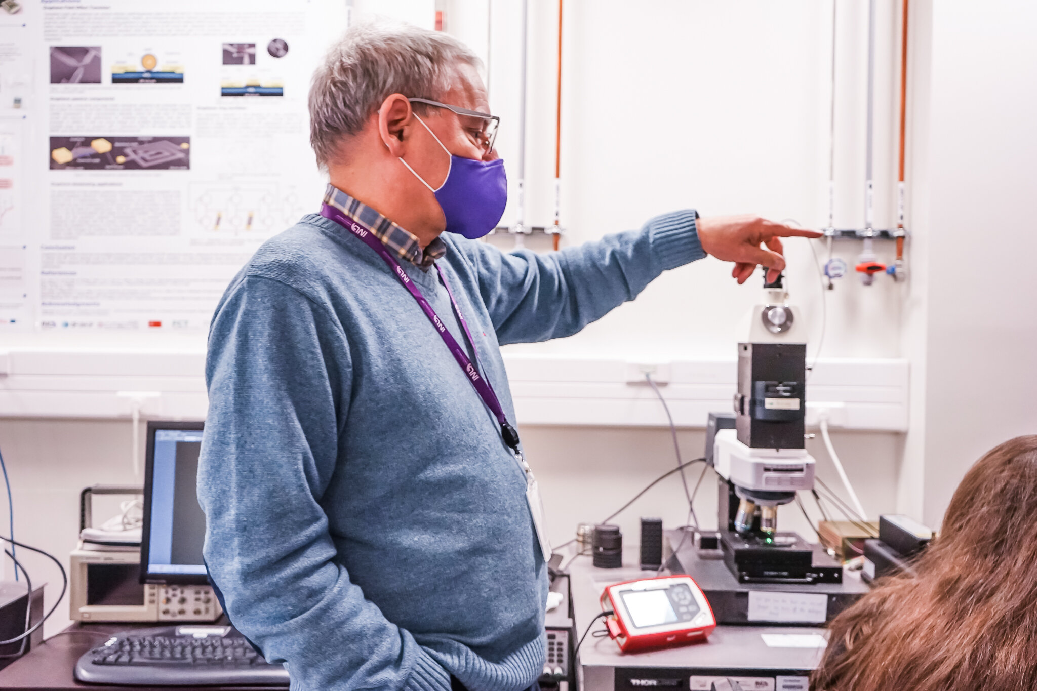
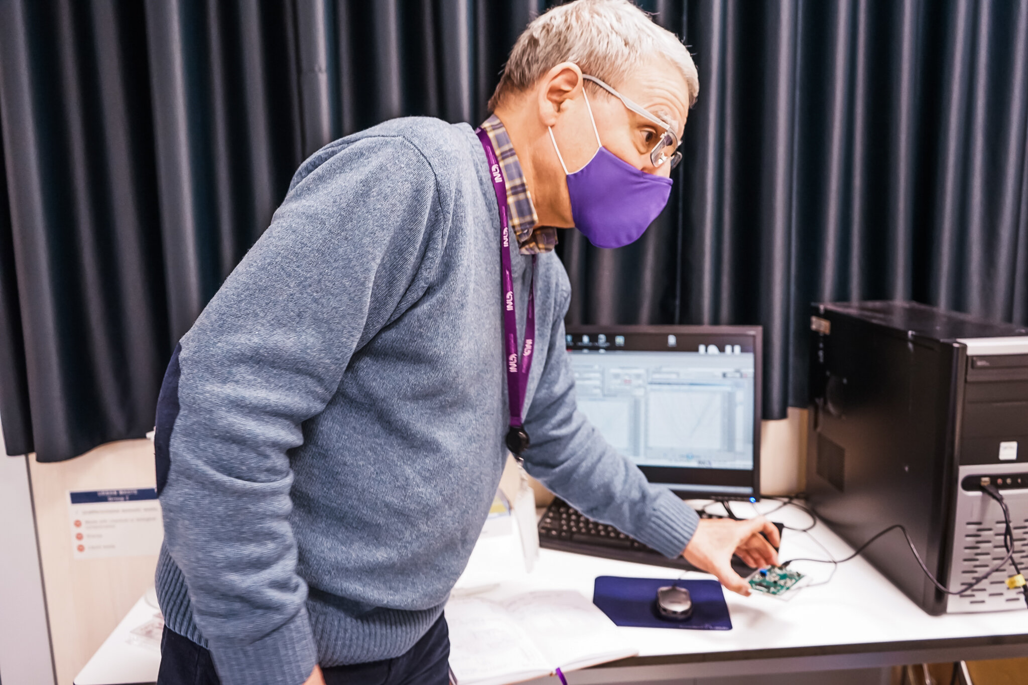
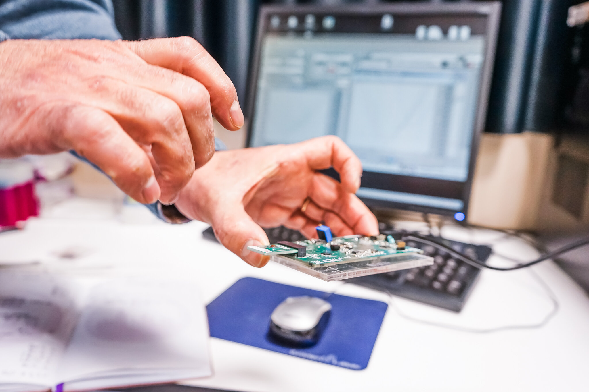
Scalable techniques to produce graphene and new practical applications, an interview with INL Group Leader, Pedro Alpuim
Pedro Alpuim is the 2D Materials and Devices Group Leader at INL. He works in CVD and 2D materials device fabrication, with an emphasis on biosensors. In particular, he develops graphene devices to detect biomarkers for medicine and environmental monitoring.
He received a PhD degree in Materials Engineering from IST Lisbon in 2003, working in amorphous silicon thin-film devices for flexible electronics, and an MSc in Physics from the UM and has published more than 90 papers in peer-reviewed journals and has h-index=24.
Can you tell us about your professional journey before arriving at INL, and what were the most important projects you’ve worked on?
I arrived at INL coming from the University of Minho, where I was (and still am) a professor in the Physics Department and before coming to INL, I installed a thin-film solar cell and semiconductor research lab at the University of Minho, in Guimarães.
Interestingly, that lab – including high-vacuum deposition systems for CVD, e-beam and thermal evaporation, and a semiconductor optoelectronic characterisation facility – was built with research equipment ceded by EU institutions based on trust and friendship at zero cost. I started to build that international scientific network during my PhD years working in flexible electronics at INESC-MN and IST, Lisbon, in Prof. João Pedro Conde’s group.
Before that, I worked as an MSc student in the KFA Jülich, Germany, in thin films’ mechanical properties, my first international experience as a scientist. Earlier, I was a secondary school teacher of physics and chemistry, which taught me how to communicate science to young people. Even earlier, I worked in a family-owned estate in wine production – Vinho Verde – helping to convert a centuries-old technology into a modern one. It was fascinating and, being then a physics student, opened my mind to the incredible richness of chemistry and biochemistry.
How did 2D Materials and Devices group start, and how does the group correlates with INL’s Research Strategy?
I arrived at INL in 2011 as a researcher from the Department of Physics of the UMinho to start applied research in graphene. Graphene was a new 2D material discovered some years before by Geim and Novoselov in 2004. In 2011, much of the incredible physics of graphene had already been elucidated, but graphene was known mainly by physicists and produced in a purely artisanal way in university labs by PhD students and post-docs using scotch tape. So the idea at INL was to develop scalable techniques to produce graphene and find a few practical applications based on its unique properties.
The first task I had at INL was to launch international tenders to purchase equipment to produce graphene. I then met Jérôme Borme, whom INL had hired before the Braga campus was finished, and was sent to Germany for an internship on graphene growth on metallic surfaces. We started the 2D materials and devices group that I first called the ‘Thin Film Devices Group’ since both Jérôme and I were in thin-film devices, magnetic devices, in his case, and in semiconductor devices. A few years later, when the laboratory was already equipped for graphene growth by CVD, and we had developed the first clean-room processed graphene wafers, the group’s name changed to 2D Materials and Devices. By then, we were also growing h-BN and planning to start working in transition-metal di-chalcogenides (MoS2 and 2MoSe2).
In 2015, we received a visitor from the Universidade Federal de São Paulo, Brazil – Nirton Vieira – who came with the idea of using our graphene in bio applications. Together, we developed the first electrolyte gate graphene transistors, which successfully detected biomolecules in solution. That strategy was particularly well aligned with the INL program in biomedicine. Motivated by these preliminary results, we started to work with Elisabete Fernandes from the INL Nanodevices group to functionalize graphene surfaces for immunoassays.
Shortly after, an electrochemist with a background in DNA sensors – Rui Campos – was hired to help develop the first graphene nanosensors. With those, we obtained a record limit of detection in the attomolar range of a 25-mer DNA sequence. We are now engaged in several projects developed around our graphene FET biosensors, from detecting counterfeiting in Port wines to Malaria or ischemic stroke early detection and neural interfaces for neurotransmission probing.
Meanwhile, the group has grown, and we now have Andrea Capasso coordinating the effort on the growth of hBN and MoSe2 for photonic and optoelectronic applications, including quantum computing technologies. Graphene conductive inks based on liquid-phase exfoliation of graphite for application in Li-ion batteries, electromagnetic interference shielding, and touch screen displays result from collaborative projects, also lead by Andrea. Two post-docs – Alexandre Chícharo and Juan Luis Pomar, this one with an individual Marie Curie fellowship – joined the group to work in plasmonic effects in 2D materials and their heterostructures. The group permanently welcomes students that work in the topics mentioned above as part of their MSc or PhD thesis.
How do you evaluate the challenges and opportunities concerning future developments in the 2D Materials area?
2D materials have a considerable potential to replace conventional 3D materials and thin films wherever physics or chemistry at an interface is critical for an application or device to succeed. Examples can be found in fields as diverse as chemical and biosensors to catalysis and nanoelectronics. The reason is that because they are purely surface, 2D materials don’t have reconstruction and dangling bond defects that are inevitable in their 3D counterparts’ surfaces.
We now have an extensive list of 2D materials obtained either by exfoliation or by CVD and other upscalable techniques, with properties that range from semi-metallic to semiconductor and dielectric. Recent developments in the field relied on the absence of surface defects in a new type of device consisting of a stack of 2D materials interconnected by weak van der Waals forces, alternating those layers with obtaining a type and level of performance impossible with conventional materials. Examples are photodetectors, magnetic topological insulators, spintronic devices, or nonvolatile memories.
More recently, a new field, known as twistronics, is emerging, where the coupling between two similar 2D layers stacked with precise control of the rotation in-plane orientation between them produces strong coupling between the electrons from both layers, giving rise to Moiré patterns that contain new physics only depending on the twisting angle. The most famous example is superconductivity in twisted bilayer graphene at the ‘magic angle’ of 1.
Briefly, what moves you about your work?
What mainly excites me about my work is the opportunity to every day having more insight and control of the properties of matter at a scale so small that it was only conceivable by the most daring spirits only a few decades ago.
To understand Nature is a formidable challenge – possibly not achievable in total, not in a lifetime for sure – but to give even little steps in that direction using the most recent and advanced technology ever fabricated by humankind is a great privilege.
And then, if one can engineer, based on that knowledge, devices, and new technologies that will help solve societal needs in innovative ways, that is the icing on the cake.
INL hosts the new event on EIT Strategy to power Europe’s largest innovation network
INL – International Iberian Nanotechnology Laboratory is hosting an event on 14 June 2021 to mark the launch of the EIT’s new strategy as part of Horizon Europe together with the European Institute of Innovation and Technology (EIT), in collaboration with the Portuguese Presidency of the Council of the European Union.
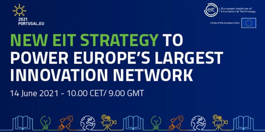
This event will have a hybrid format and can be attended either online or in person at the International Iberian Institute of Nanotechnology (INL), in Braga, Portugal.
With an enhanced mandate and a budget of EUR 2.9 billion for 2021 to 2027, the EIT will help drive the recovery of the economy as well as Europe’s green and digital transition for a more sustainable and resilient society.
The new EIT strategy has four main priorities and many new features. It will enable the EIT Community to strengthen its impact, boost its support to higher education and increase its regional development efforts. The EIT will also set up two new EIT Knowledge and Innovation Communities: the first in 2022 in the field of the Cultural and Creative Sectors and Industries and the second in the field of water, marine and maritime sectors and ecosystems in 2026.
The event is open to innovators, entrepreneurs and organisations from business, education and research who want to learn more about the EIT and the different opportunities to innovate with the EIT Community. It will be interactive, and participants will be able to join discussions through Q&As, polls and social media.
Among the prominent speakers, you will hear from Mariya Gabriel, European Commissioner for Innovation, Research, Culture, Education and Youth; Manuel Heitor, Portuguese Minister of Science, Technology and Higher Education and Gioia Ghezzi, Chair of the EIT Governing Board.
You can check the full programme by clicking here.
EURONANOFORUM: Using Nanotechnologies and Advanced Materials to create a future together

The Day 1 of the EuroNanoForum brought the commitment of the European Commission towards a strong investment and support to Nanotechnology and Advanced Materials, as crucial elements of Europe’s recovery and resilience.
EU Commissioner Mariya Gabriel and Director of Prosperity Peter Dröll were unequivocal in assuring all the conference participants that the challenge is accepted.
The first-day sessions also brought key insights to the table regarding what needs to be done to place Europe in a relevant position in the global scene again.
The interaction between academia and industry was identified as the decisive link to make innovation happen and scale up the research results from the labs to the market.
The 2021 edition of the EuroNanoForum ended with a second day full of new insights about what Europe needs to recover, thrive, and become more resilient, with the support of Nanotechnology and Advanced Materials.
The effects of the pandemic were discussed in almost every session, not only because of its devastating effects but also for the revealing effect it had in the way we must do everything from now on.
It became clear that the transition to a green and sustainable economy cannot be done without Nanotechnology, and also that Europe needs Advanced Materials to drive innovation while creating opportunities to develop its markets, products, and services if it wants to become competitive.
Another key take-out of this EuroNanoForum was the demonstration that Research and Industry need to be more aligned than ever to make innovation a reality, by connecting the dots and finding a common ground.
Another connection that needs to be improved is the one between the public and the private sector, and even more in a moment when Europe needs to properly channel a significant amount of financial support to the right initiatives so that the investment is made in the fields that matter and can promote a change for the better.
In the closing session, both the Director-General of INL, Lars Montelius, who hosted the EuroNanoForum 2021 and the Director of Prosperity at the European Commission, Peter Dröll, agreed that “it’s all about the people, the planet and prosperity. It is our work to make this the best place to be, using Nanotechnologies and Advanced Materials to create a future together”.
As Clare Skentlebery, one of the speakers in Plenary Session 3 (Recovery Plan for Europe) well put it, “Alone you go fast. Together you go further”. The EuroNanoForum 2021 gathered a total of 3640 participants from over 140 countries, providing thousands of opportunities for networking and collaboration through almost 200 scientific posters, 17 exhibitors, five satellite events, and several hours of sessions about topics that the European Nanotechnology community is now even more empowered to intervene upon.
Next Page » « Previous Page -->The Day 1 of the EuroNanoForum brought the commitment of the European Commission towards a strong investment and support to Nanotechnology and Advanced Materials, as crucial elements of Europe’s recovery and resilience.
EU Commissioner Mariya Gabriel and Director of Prosperity Peter Dröll were unequivocal in assuring all the conference participants that the challenge is accepted.
The first-day sessions also brought key insights to the table regarding what needs to be done to place Europe in a relevant position in the global scene again.
The interaction between academia and industry was identified as the decisive link to make innovation happen and scale up the research results from the labs to the market.
The 2021 edition of the EuroNanoForum ended with a second day full of new insights about what Europe needs to recover, thrive, and become more resilient, with the support of Nanotechnology and Advanced Materials.
The effects of the pandemic were discussed in almost every session, not only because of its devastating effects but also for the revealing effect it had in the way we must do everything from now on.
It became clear that the transition to a green and sustainable economy cannot be done without Nanotechnology, and also that Europe needs Advanced Materials to drive innovation while creating opportunities to develop its markets, products, and services if it wants to become competitive.
Another key take-out of this EuroNanoForum was the demonstration that Research and Industry need to be more aligned than ever to make innovation a reality, by connecting the dots and finding a common ground.
Another connection that needs to be improved is the one between the public and the private sector, and even more in a moment when Europe needs to properly channel a significant amount of financial support to the right initiatives so that the investment is made in the fields that matter and can promote a change for the better.
In the closing session, both the Director-General of INL, Lars Montelius, who hosted the EuroNanoForum 2021 and the Director of Prosperity at the European Commission, Peter Dröll, agreed that “it’s all about the people, the planet and prosperity. It is our work to make this the best place to be, using Nanotechnologies and Advanced Materials to create a future together”.
As Clare Skentlebery, one of the speakers in Plenary Session 3 (Recovery Plan for Europe) well put it, “Alone you go fast. Together you go further”. The EuroNanoForum 2021 gathered a total of 3640 participants from over 140 countries, providing thousands of opportunities for networking and collaboration through almost 200 scientific posters, 17 exhibitors, five satellite events, and several hours of sessions about topics that the European Nanotechnology community is now even more empowered to intervene upon.