News

INL involved in EC´s coordinated approach to promote the safety of nanomaterials

INL involved in EC´s coordinated approach to promote the safety of nanomaterials

The International Iberian Nanotechnology Laboratory (INL) participates in the European Commission’s NANoREG project on the safety of nanomaterials. At INL, the goal of this four-year project is to establish and test specific measurement and characterization methods and offer a wide set of well‐characterized manufactured or engineered nanomaterials (MNMs). The industrial use of nanomaterials has grown significantly, therefore more knowledge about the health and environmental hazard impacts of nanomaterials is necessary. Interest in the use of nanomaterials is considerable, as they can be used to improve product characteristics; for example, nanoparticles help make a surface self-cleaning through a hydrophobic coat of paint; but the safety of these nanoparticles raises questions. The fast development of nanomaterials and their presence on the market make it necessary to evaluate their environmental and health impacts. The project aims at developing guidelines for safe usage, risk management and safety instructions while assessing the need for new legislation. NANoREG is a FP7 project aiming to deliver the answers needed by regulators and legislators on EHS by linking them to scientific evaluation of data and test methods. The NANoREG consortium joins governmental authorities, research institutes and companies from 14 European countries. With this project, we will get not […]

Read more

INL project presented during EU Open Days Week in Brussels

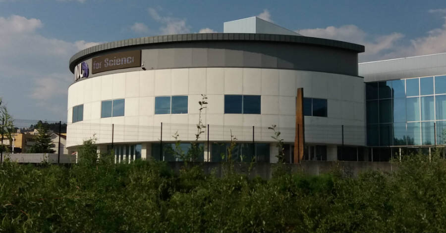
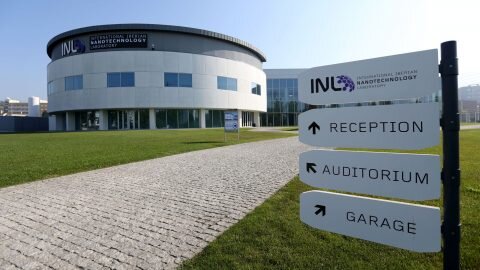
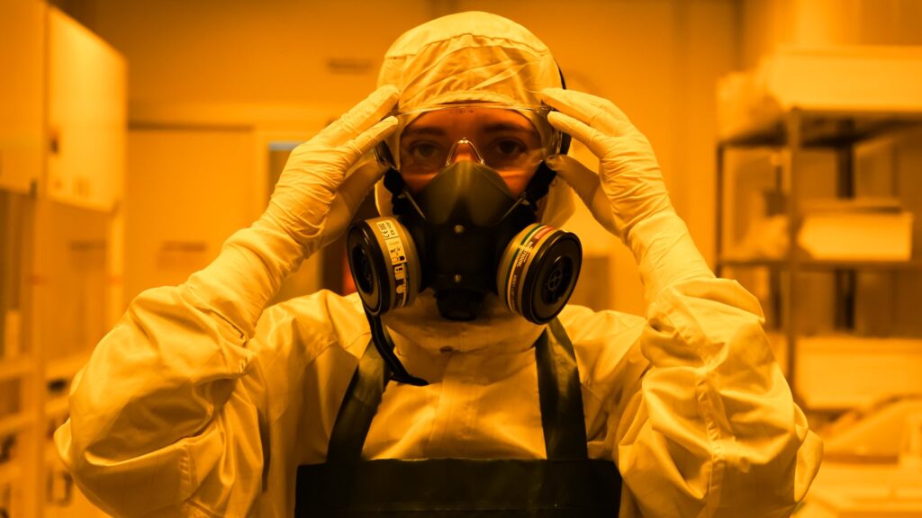
The INL – International Iberian Nanotechnology Laboratory project was presented during this year’s EU Open Days seminars, by its director-general, José Rivas, included in the panel «Cross-border cooperation boosts innovation», this month (October), in Brussels. The main objective of the project was building a centre of excellence in applied nanotechnology research, with a positive impact in the region’s competitiveness, promotions of qualified employment, creations of companies, but also in the development of the relational model Administration/INL/Company/University. The project submitted by INL comprised the construction of competitive scientific infrastructures, with the objective to attract top researchers in the field of nanotechnology. The installation of the facilities in the North of Portugal, more precisely in Braga, favoured the development of methodologies that enhance an ecosystem of spin-offs, as well as the integration of the INL in Networks of knowledge. The region benefits now from a competitive technological infrastructure, on an international level, increasing the regional competitiveness of companies, universities and technological centres. The construction of the INL facility was co-financed in 30 million euros, by the Cross-Border Cooperation Programme Spain Portugal 2007-2013, through the ERDF (European Regional Development Fund) . The INL project falls under Priority Axis I «Strengthen Competitiveness and Promoting […]

Read more
Workshop on Nanotechnology in Food at INL

Workshop on Nanotechnology in Food at INL

The International Iberian Nanotechnology Laboratory (INL) hosted an International Workshop on Nanotechnology Applications in Food – Challenges and Opportunities, last September 3rd and 4th, in Braga. This two-day workshop aimed to present the impact of nanotechnology in the food sector. The potential applications of Nanotechnology in subjects such as food safety, traceability, packaging performance and processing, among others, are expected to significantly improve the quality of food products in the near future. With the development of Nanotechnology, new nanoscale science, materials and structures, and nano-enabled devices and systems can be very beneficial and important in the food industry. The meeting enabled attendants to hear opinions from experts on nanotechnology applied to the food sector. For more information, please contact isabel.machado(at)inl.int

Read more
Ministers of Science of Portugal and People’s Republic of China visited the INL

Ministers of Science of Portugal and People’s Republic of China visited the INL

The Portuguese Minister of Education and Science of Portugal, Nuno Crato, and the Minister of Science and Technology, of the People’s Republic of China, Wan Gang, visited the International Iberian Nanotechnology Laboratory. After a short meeting with the aim of presenting to the Chinese delegation the INL project, a state-of-the-art facility, fully dedicated to nanotechnology and nanosciences, the two ministers visited the laboratories dedicated to nanomaterial’s, energy storage and conversion, nanochemistry and nanoparticle synthesis , spintronics and magnetometry. In the last two laboratories the Chinese Minister of Science had the chance to meet two Chinese researchers who are developing their work at INESC-MN, in collaboration with INL. The tour through the facilities, guided by INL’s the director-general, José Rivas, and deputy director general, Paulo Freitas included also the high accuracy laboratories where the Minister of Science and Technology Wan Gang took a closer look at the transmission electron microscopy (TEM), the scanning electron microscopy (STEM), as well as the focus ion beam (FIB). Nanotechnology is one of the areas included in the memorandum of understanding signed between the government of People’s Republic of China and Portugal to promote collaborative research.

Read more
FINLAND OPEN TO ACADEMIC AND INDUSTRIAL COLABORATION IN NANOTECHNOLOGY

FINLAND OPEN TO ACADEMIC AND INDUSTRIAL COLABORATION IN NANOTECHNOLOGY

The Director-General of the International Iberian Nanotechnology Laboratory (INL), José Rivas, was pleased with the interest shown by the Finish academic and industrial institutions visited during the stay organized by the President of the Republic of Portugal, Aníbal Cavaco Silva, to Helsinki, last week. Erkki Ormala, Vice-President for Business Environment at Nokia, one of the world leaders in communication technologies, showed interest in visiting the International Iberian Nanotechnology Laboratory, with its headquarters in Braga. The future visit of Nokia representatives will allow establishing collaborations in strategic areas like electronic devices and sensors. INL also visited Micronova, the Centre for Micro and Nanotechnology Nanofabrication, on the Otaniemi Campus of Aalto University, where the delegation was hosted by Ilkka Niemela, Dean of the School of Science. The Research, Technology and Development activities of the finish nanotechnology cluster were made known through several presentations. From these presentations, Prof. Rivas concluded that there are groups of excellence working on nanomedicine and materials research. «The academic quality is remarkable and the way research and industry are connected in an example to be considered», said José Rivas. One of the strategic goals of INL is to stand out as a scientific organization of excellence, with an […]

Read more
INL installs LPX Pegasus ASE, a Deep Silicon Etch (DRIE) with a broad range of challenging applications

INL installs LPX Pegasus ASE, a Deep Silicon Etch (DRIE) with a broad range of challenging applications

Advanced Silicon Etch (ASE) is a deep reactive ion etching (DRIE) technique used to rapidly etch deep and high aspect ratio structures in silicon. LPX Pegasus is the continuation of STS’ Advanced Silicon Etch (ASE) technology. Through an in-depth understanding of the Bosch process and with the required hardware, Pegasus is able to provide excellent profile control and selectivity. The increased etch rate and improved uniformity lead to higher throughput and device yield, resulting in increased productivity. This inductively de-coupled plasma (IDP) system uses fluorine-based gases for anisotropic deep silicon trench etching. The 13.56 MHz RF power supply produces high-density, low-pressure, low-energy plasma. This type of plasma allows high selectivity and aspect ratio etching for depths greater than 150 microns and has an expected etch rate better than 15 microns/ min. Used primarily for MEMs devices, the typical materials used in this etcher are silicon wafers covered with photoresist and thin films of silicon dioxide and silicon nitride. The performance improvements that Pegasus brings have numerous benefits for research as well as for end-users. At the moment, the tool is being installed in the INL’s facilities and it is expected that the final validation process will take place the first […]

Read more
1 47 48 49