News

Ministers of Science of Portugal and People’s Republic of China visited the INL

Ministers of Science of Portugal and People’s Republic of China visited the INL

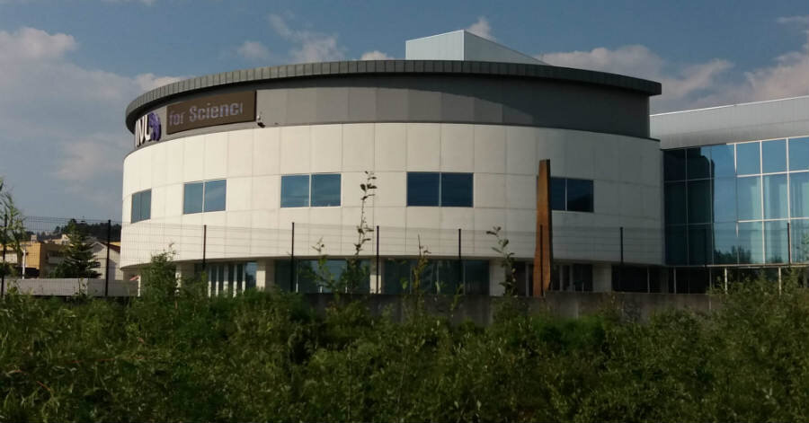
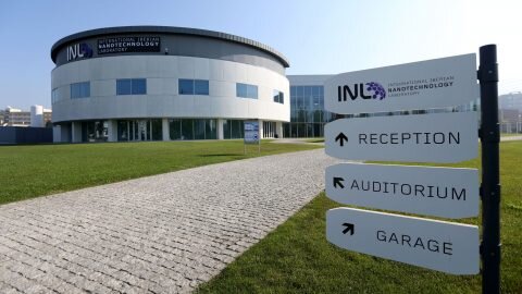
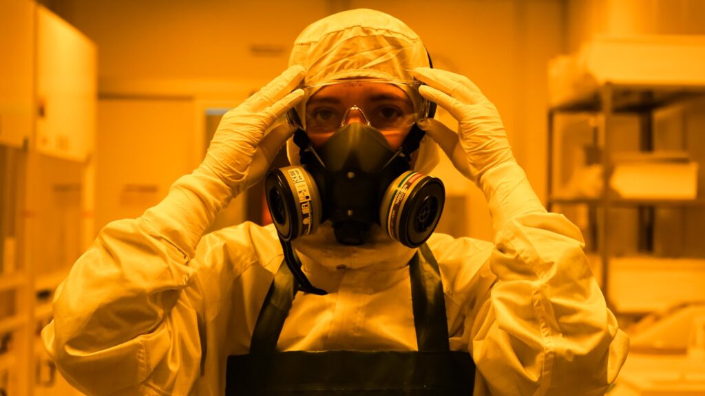
The Portuguese Minister of Education and Science of Portugal, Nuno Crato, and the Minister of Science and Technology, of the People’s Republic of China, Wan Gang, visited the International Iberian Nanotechnology Laboratory. After a short meeting with the aim of presenting to the Chinese delegation the INL project, a state-of-the-art facility, fully dedicated to nanotechnology and nanosciences, the two ministers visited the laboratories dedicated to nanomaterial’s, energy storage and conversion, nanochemistry and nanoparticle synthesis , spintronics and magnetometry. In the last two laboratories the Chinese Minister of Science had the chance to meet two Chinese researchers who are developing their work at INESC-MN, in collaboration with INL. The tour through the facilities, guided by INL’s the director-general, José Rivas, and deputy director general, Paulo Freitas included also the high accuracy laboratories where the Minister of Science and Technology Wan Gang took a closer look at the transmission electron microscopy (TEM), the scanning electron microscopy (STEM), as well as the focus ion beam (FIB). Nanotechnology is one of the areas included in the memorandum of understanding signed between the government of People’s Republic of China and Portugal to promote collaborative research.

Read more
FINLAND OPEN TO ACADEMIC AND INDUSTRIAL COLABORATION IN NANOTECHNOLOGY

FINLAND OPEN TO ACADEMIC AND INDUSTRIAL COLABORATION IN NANOTECHNOLOGY

The Director-General of the International Iberian Nanotechnology Laboratory (INL), José Rivas, was pleased with the interest shown by the Finish academic and industrial institutions visited during the stay organized by the President of the Republic of Portugal, Aníbal Cavaco Silva, to Helsinki, last week. Erkki Ormala, Vice-President for Business Environment at Nokia, one of the world leaders in communication technologies, showed interest in visiting the International Iberian Nanotechnology Laboratory, with its headquarters in Braga. The future visit of Nokia representatives will allow establishing collaborations in strategic areas like electronic devices and sensors. INL also visited Micronova, the Centre for Micro and Nanotechnology Nanofabrication, on the Otaniemi Campus of Aalto University, where the delegation was hosted by Ilkka Niemela, Dean of the School of Science. The Research, Technology and Development activities of the finish nanotechnology cluster were made known through several presentations. From these presentations, Prof. Rivas concluded that there are groups of excellence working on nanomedicine and materials research. «The academic quality is remarkable and the way research and industry are connected in an example to be considered», said José Rivas. One of the strategic goals of INL is to stand out as a scientific organization of excellence, with an […]

Read more
INL installs LPX Pegasus ASE, a Deep Silicon Etch (DRIE) with a broad range of challenging applications

INL installs LPX Pegasus ASE, a Deep Silicon Etch (DRIE) with a broad range of challenging applications

Advanced Silicon Etch (ASE) is a deep reactive ion etching (DRIE) technique used to rapidly etch deep and high aspect ratio structures in silicon. LPX Pegasus is the continuation of STS’ Advanced Silicon Etch (ASE) technology. Through an in-depth understanding of the Bosch process and with the required hardware, Pegasus is able to provide excellent profile control and selectivity. The increased etch rate and improved uniformity lead to higher throughput and device yield, resulting in increased productivity. This inductively de-coupled plasma (IDP) system uses fluorine-based gases for anisotropic deep silicon trench etching. The 13.56 MHz RF power supply produces high-density, low-pressure, low-energy plasma. This type of plasma allows high selectivity and aspect ratio etching for depths greater than 150 microns and has an expected etch rate better than 15 microns/ min. Used primarily for MEMs devices, the typical materials used in this etcher are silicon wafers covered with photoresist and thin films of silicon dioxide and silicon nitride. The performance improvements that Pegasus brings have numerous benefits for research as well as for end-users. At the moment, the tool is being installed in the INL’s facilities and it is expected that the final validation process will take place the first […]

Read more
1 75 76 77